


All Products
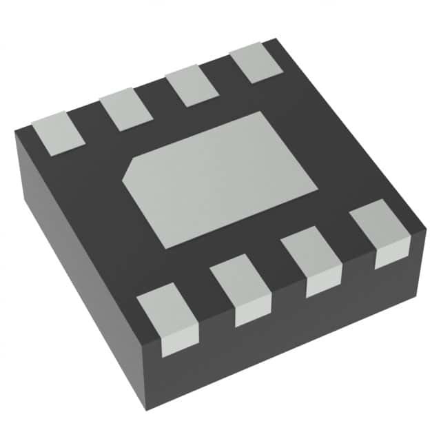
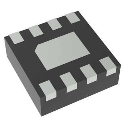
Surface Mount Clock Timing IC NB3L553MNR4G 200MHZ 8DFN onsemi
| Brand Name | onsemi |
|---|---|
| Model Number | NB3L553MNR4G |
| Minimum Order Quantity | 1 |
| Price | Based on current price |
| Packaging Details | anti-static bag & cardboard box |
| Delivery Time | 3-5 work days |
| Payment Terms | T/T |
| Supply Ability | In stock |
Product Details
| Type | Fanout Buffer (Distribution) | Number Of Circuits | 1 |
|---|---|---|---|
| Ratio - InputOutput | 1:4 | Differential - InputOutput | No/No |
| Input | LVCMOS, LVTTL | Output | LVCMOS, LVTTL |
| Frequency - Max | 200 MHz | Voltage - Supply | 2.375V ~ 5.25V |
| Operating Temperature | -40°C ~ 85°C | Mounting Type | Surface Mount |
| Package / Case | 8-VFDFN Exposed Pad | Supplier Device Package | 8-DFN (2x2) |
| Highlight | Surface Mount Clock Timing IC,Clock Timing IC 200MHZ,NB3L553MNR4G |
||
Product Description
NB3L553MNR4G IC CLK BUFFER 1:4 200MHZ 8DFN onsemi
Product Details
Description
The NB3N511 is a clock multiplier that will generate one of nine selectable output multiples of an input frequency via two 3−level select inputs (S0, S1). It accepts a standard fundamental mode crystal or an external reference clock signal. Phase−Locked−Loop (PLL) design techniques are used to produce a low jitter, TTL level clock output up to 200 MHz with a 50% duty cycle. An Output Enable (OE) pin is provided, and when asserted low, the clock output goes into tri−state (high impedance). The NB3N511 is commonly used in electronic systems as a cost efficient replacement for crystal oscillators
Features
• Clock Output Frequencies up to 200 MHz• Nine Selectable Multipliers of the Input Frequency
• Operating Range: VDD = 3.3 V ±10% or 5.0 V ±5%
• Low Jitter Output of 25 ps One Sigma (rms)
• Zero ppm Clock Multiplication Error
• 45% − 55% Output Duty Cycle
• TTL/CMOS Output with 25 mA TTL Level Drive
• Crystal Reference Input Range of 5 − 32 MHz
• Input Clock Frequency Range of 1 − 50 MHz
• OE, Output Enable with Tri−State Output
• 8−Pin SOIC
• Industrial Temperature Range −40°C to +85°C
• These are Pb−Free Devices
Specifications
| Attribute | Attribute Value |
|---|---|
| Manufacturer | onsemi |
| Product Category | Clock Buffers, Drivers |
| Series | NB3L553 |
| Type | Fanout Buffer (Distribution) |
| Packaging | Alternate Packaging |
| Unit-Weight | 0.001344 oz |
| Mounting-Style | SMD/SMT |
| Package-Case | 8-VFDFN Exposed Pad |
| Operating-Temperature | -40°C ~ 85°C |
| Mounting-Type | Surface Mount |
| Voltage-Supply | 2.375 V ~ 5.25 V |
| Supplier-Device-Package | 8-DFN (2x2) |
| Input | LVCMOS, LVTTL |
| Output | LVCMOS, LVTTL |
| Number-of-Circuits | 1 Circuit |
| Ratio of output to input | 1899/12/30 1:04:00 |
| Differential-Input:Output | No/No |
| Frequency-Max | 200MHz |
| Number-of-Outputs | 4 Output |
| Maximum Operating Temperature | + 85 C |
| Operating temperature range | - 40 C |
| Supply-Voltage-Max | 5.25 V |
| Supply-Voltage-Min | 2.375 V |
| Package-Case | DFN-8 EP |
| Maximum-Input-Frequency | 200 MHz |
| Propagation-Delay-Max | 5 ns 4 ns |
Descriptions
Clock Fanout Buffer (Distribution) IC 1:4 200MHz 8-VFDFN Exposed Pad
Clock Fanout Buffer 4-OUT 1-IN 1:4 Automotive 8-Pin DFN EP T/R
Clock Buffer 1:4 Clock Buffer 2.5/3.3/5 V
Recommended Products